Latest about Software

Devs defend PHP programming language despite dip in popularity
News Supporters of the PHP programming language insist there are still plenty of cool projects being built with it, but it's popularity has waned in recent years

Google Workspace Review
Reviews From free to enterprise, Google’s ever-popular productivity suite has a range of tiers and functions for all sizes of business
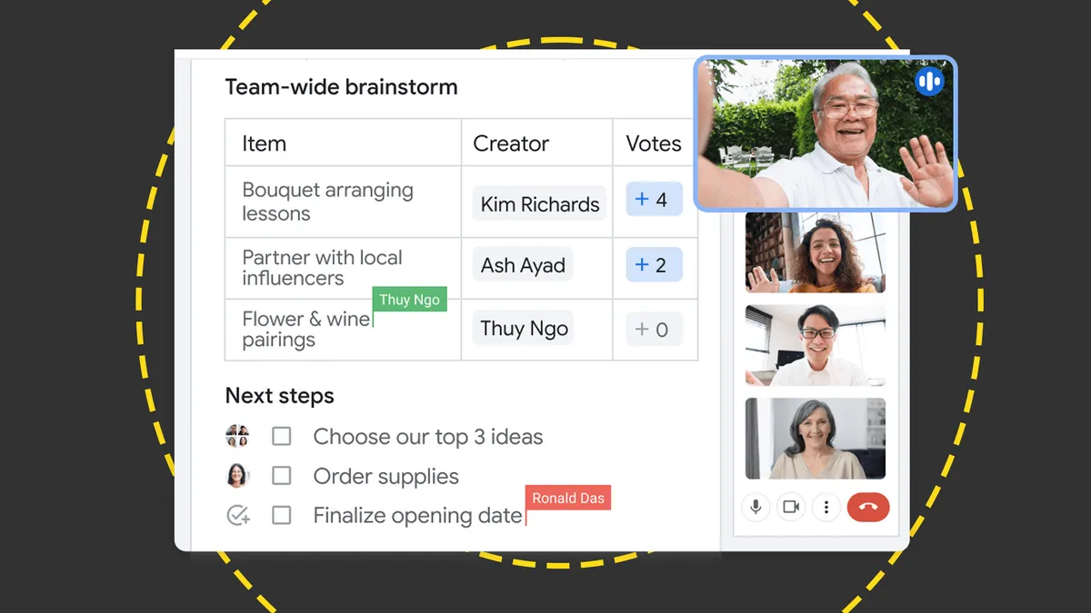
One of our favorite productivity suites of 2023 just got a bunch of new AI tools — but they come with a steep price tag
News Updates to Google Workspace are designed to reduce pressure around taking notes and let workers be more engaged during meetings and calls

Why Flux CD’s survival is another major victory for the open source community
News Despite a rocky road after the fall of Weaveworks, Flux CD is now receiving support from several organizations

Linux Foundation unveils Redis alternative, 'Valkey', with backing from AWS, Google Cloud, and Oracle
News Valkey will provide developers with an open source Redis alternative following the firm’s move to a more restrictive licensing scheme in March

Trello for business: A complete guide to managing your workflows
Tutorials From the free tier to the enterprise version, ITPro talks you through your Trello workflow, from start to finish
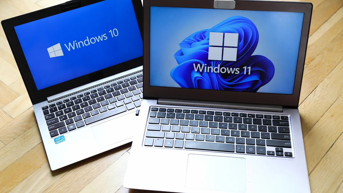
New Windows 10 prices show Microsoft is getting desperate in pushing users to the latest operating system
News The firm has extended support for the operating system, but the hefty price tags show it’s keen to push users to Windows 11

Google devs ditched C++ for Rust — here's what happened
News Rust developers are twice as productive as their counterparts using other programming languages such as C++