Scientists create nanowires only three atoms wide
Invention could result in thinner and smaller devices

Nanowires measuring three atoms in thickness have been created by US researchers, paving the way for smaller processors and thinner gadgets in the future.
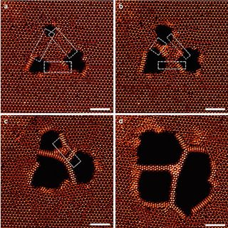
A team working at the Oak Ridge National Laboratory in Tennessee created the world's thinnest wires using a beam of electrons.
The team was lead by Junhao Lin, a Vanderbilt University PhD student and visiting scientist at the laboratory. The project was backed by funding from the US Department of Energy Office of Science.
The flexible, thin wires are one thousandth of the size of the ones that connect transistors in modern electronics.
According to his advisor Sokrates Pantelides, University Distinguished Professor of Physics and Engineering at Vanderbilt University, the technique represents a new way to manipulate matter at the nanoscale and should boost efforts to create electronic circuits out of atomic monolayers, the thinnest possible form factor for solid objects.
Lin and his team whittled out the wires from transition-metal dichalcogenides (TMDCs). Combining the metals molybdenum or tungsten with either sulfur or selenium makes these TMDCs.
These form atomic monolayers, which are highly sought after by the electronics industry for their exceptional strength and flexibility, transparency and high electron mobility.
Get the ITPro. daily newsletter
Receive our latest news, industry updates, featured resources and more. Sign up today to receive our FREE report on AI cyber crime & security - newly updated for 2024.
While other monolayer material, such as graphene, has these characteristics, so far scientists have had trouble converting them into useful devices. While other research groups have already created functioning transistors and flash memory gates out of TMDC materials, this latest discovery provides a means for interconnecting these basic elements.
"This will likely stimulate a huge research interest in monolayer circuit design," Lin said. "Because this technique uses electron irradiation, it can - in principle - be applicable to any kind of electron-based instrument, such as electron-beam lithography."
While the research is still in its early stages, Pantelides said: "If you let your imagination go, you can envision tablets and television displays that are as thin as a sheet of paper that you can roll up and stuff in your pocket or purse."
Lin sad the new technique could make it possible to create three-dimensional circuits by stacking monolayers "like Lego blocks" and using electron beams to fabricate the wires that connect the stacked layers.
More information on the technique can be found in the latest edition of the journal Nature Nanotechnology.
Rene Millman is a freelance writer and broadcaster who covers cybersecurity, AI, IoT, and the cloud. He also works as a contributing analyst at GigaOm and has previously worked as an analyst for Gartner covering the infrastructure market. He has made numerous television appearances to give his views and expertise on technology trends and companies that affect and shape our lives. You can follow Rene Millman on Twitter.
Most Popular


