A deep-dive into AMD Epyc Rome: Meet the Zen 2 server chips
AMD has finally launched its second-gen Epyc processors, codenamed Rome. Here’s how the Red Team has built them

Two years after AMD made its server processor comeback with its Zen architecture Epyc chips, it's now launched a new family of second-generation Epyc parts - codenamed Rome - at a series of events in San Francisco.
Of course, we've known quite a lot about Rome - from its 7nm manufacturing process, a first for server processors, to its unique 'hybrid' die layout - since it was first announced in November 2018. The launch festivities, however, have given us our most detailed look yet at both the range of chips and how they work.
Epyc second generation: Hardware
As we already knew, the new Epyc processors use AMD's Zen 2 architecture, which is based on a tiny 7nm process. In fact, these are the very first high-performance 7nm x86 CPUs of their kind, compared to the 14nm process used by Intel's Xeon server chips.
Having a more compact manufacturing process than the 14nm Zen architecture has conferred numerous benefits, according to AMD. The first is that its greater efficiency has allowed for faster clock speeds, so whereas only a single first-generation part - the Epyc 7371 - had a base clock speed higher than 3GHz, three of the new lineup get this honor. Maximum boost clocks range from 3.2GHz to 3.4GHz, another broad improvement (excluding the Epyc 7371, which could hit 3.8GHz).
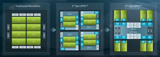
The smaller process has given AMD enough physical room to make drastic changes to each processor's layout. Rome's "chiplet" design differs from that of the first Epyc parts, which in turn differs from traditional monolithic designs. This time, rather than have groups of core clusters with their own memory and I/O controllers, Rome's 'hybrid multi-die' includes a single centralised I/O die, with the 7nm chiplets shooting off from it.

As such, each chiplet gets equal access to all eight DDR4 channels (the number of channels remains unchanged, though faster DDR4-3200 memory is now supported), cutting the latency you'd otherwise get accessing a channel that isn't part of the same module as the core cluster. It's also a highly modular system - AMD can simply occupy more chiplet spots or leave them empty - which might help explain why, with 14 second-generation Epyc processors launching, there are so many.
In dual-socket setups, the centralised design also promises to cut NUMA (non-uniform memory access) latency. On the original Epyc layout, there'd be three NUMA domains with three different distances between them; on the new design, there are only two domains and two distances, the latter both being shorter than the two longest distances of the three on the first generation. Average latency is lower as a result.
Get the ITPro. daily newsletter
Receive our latest news, industry updates, featured resources and more. Sign up today to receive our FREE report on AI cyber crime & security - newly updated for 2024.
It's also worth noting that the I/O die uses a 14nm process, on the basis that I/O doesn't benefit as much from a more efficient manufacturing process as the CPU cores.
Speaking of which, you can now get Epyc chips with up to 64 cores and 128 threads, doubling the previous maximum. 48-core, 32-core, 24-core, 16-core, 12-core and 8-core models will be available too, each with double the threads. This is likely causing some degree of nervousness to Intel, which has only just managed to announced that its upcoming Cooper Lake server chips will max out at a mere 56 cores.
Elsewhere, maximum L3 cache capacity has doubled to 256MB, though you'll only get this on the top-end 7742, 7702 and 7642 models. Floating-point width, on the other hand, has doubled for all models, up to 256-bit.

Rome chips will also be the first to support PCIe 4.0 devices. It's finally been confirmed that the number of available lanes will be the same as the first generation, 128, but that's still an awful lot for a single socket. More importantly, you'll be able to build systems with PCIe 4.0 SSDs, which aren't very numerous at the moment but can reach far higher read and write speeds than even the fastest PCIe 3.0 drives.
Epyc second generation: Performance and benchmarks
With all of these tweaks and enhancements, you'd expect quite the uptick in performance. AMD is promising around a 15% improvement in instructions per clock compared to 2017's Epyc chips, though the demos and benchmarks on show in San Francisco were far more focused on how the new parts shape up next to Intel's equivalents.
The majority of these results were simply being presented to us, though we're told they were originally recorded by independent parties instead of AMD itself. In the Microsoft SQL Server benchmark, for example, the top-of-the-line Epyc 7742 was shown performing around 8,900,000 transactions per second, while Intel's top chip - the Xeon Platinum 8280 - hovered around the 6,100,000 mark. Considering the 7742 is a 64-core chip costing $6,950 and the 8280 is a 28-core chip costing $13,012, that's quite the win for AMD, and in more ways than one.
The same processor also beat the same Intel rival in the Altair Taurus Crash Simulation, which involves simulating and recording metrics on a highly detailed virtual crash test - the 7742 did it in 2hrs 28mins, while the 8280 took 4hrs 13ms. In the SPECjbb2015 MulitJVM Max test for Java performance, AMD also quoted a score of 171,000 for the 7742 and 92,000 for the 8280.
In short, the Epyc 7742 is a very beefy processor. It's unsurprising that AMD focused on its highest-specced part, and this does mean we're still unsure of how well lesser Rome chips will perform, but what we've seen so far has been very encouraging.

That includes how the 7742 was also seemingly able to, by itself, encode live 8K video at 60fps and using the HEVC standard. This might not be the most obvious use of a server processor, but it has big implications at a time when 8K is blossoming; Epyc could provide a relatively simple and inexpensive solution for broadcasters to get live 8K footage of major events (like the Olympics or the World Cup) out on the airwaves.
Epyc second generation: Security
Rome introduces a number of new security measures, too. Memory encryption is a big one; an AES-128 encryption engine sits in front of the memory controller, and keys are managed by the onboard AMD Secure Processor. This microprocessor isn't itself a new feature, but it is being used in new ways, and here it ensures that encryption keys aren't visible to the main x86 cores.
Another addition, Secure Encrypted Virtualization, cryptographically isolates virtual machines from each other, as well as an untrusted Hypervisor. Again, this uses AES-128 encryption, and individual keys can be allocation to the hypervisor, single VMs or groups of VMs.
Rome is also hardened against Spectre attacks at the hardware level, unlike the previous Epyc chips that were only protected via firmware and/or the OS or virtual machine monitor.
Epyc second generation: Availability
For proof of what a serious challenge Epyc is mounting to Intel's server platforms, look no further than the OEM support for its second generation. Although the previous generation of Zen chips was only available in a handful of servers, HPE and Dell EMC are both tripling their AMD server portfolios, and Lenovo is introducing two new systems based on Epyc 2.
Epyc second generation: Verdict
The past few months of drip-fed details about Rome have meant that there wasn't much left to be surprised about. What these processors lack in excitement, though, they make up for in promise: if the Epyc 7742 is any indication, we could be seeing a raft of new processors that not only massively outperform their Intel counterparts, but do so for much less cash.
That's not just the initial outlay, either. True, switching to a 7nm process can help with speed and efficiency, but the odd clock speed increase here or memory optimisation there can all add up to the ability to have a server rack that does the same amount of work with fewer chips. Ultimately, that's what Epyc's second generation is all about: more cores, but fewer processors, smaller servers, and lower total costs.


